
Iridian Participates at SPIE BiOS and Photonics West in San Francisco
Members of the Iridian team will be attending SPIE’s BiOS and Photonics West events, hosted at the renowned Moscone Center in San Francisco, California. Meet us there!
Iridian is Attending InterOpto 2025
Iridian will be exhibiting in InterOpto 2025, Pacifico Yokohama, Japan, November 11-13, 2025. We will show case our Spectroscopy filters, Filters for sensing and communication networks and MWIR/LWIR filters. We look forward to seeing you at booth# B-19 to discuss your...Extra-Terrestrial Connections: Enabling Optical Mesh Networks in Orbit
As the realm above Earth’s atmosphere shifts from the domain of national space agencies to private corporations, the challenges associated with designing and deploying robust, space-based optical networks are evolving as well. In addition to meeting the rigorous technical demands of optical intersatellite links (OISL), organizations operating in space must contend with impactful commercial and supply chain considerations. Click to learn more.
Integrated Multifunction Filters Help Telecom Module Engineers Do More with Less
Explore the advantages of Iridian multifunction filters for telecom applications and their role in device miniaturization and performance.
CIOE 2025
Iridian will be visiting CIOE 2025, September 10-12, 2025. Please contact Yongbao Xin directly at yxin@idexcorp.com if you would like to book a meeting with us.
Email Change Notice
Please be advised that our previous email address, ***@iridian.ca, is no longer in use. Should you need to contact a specific individual at Iridian and are unaware of their updated email address, kindly reach out to us at istsales1@idexcorp.com for assistance.
Laser World of Photonics 2025
Iridian will be visiting Laser World of Photonics 2025 on June 24-27 in The Trade Fair Center Messe München in Germany.
If you would like to have a meeting with us at the venue, please contact Daniel Ulba (dulba@idexcorp.com) directly or send a message through our website.
How Optical Filters Enable Data Centers’ Ubiquitous AI Demands
Iridian has a wealth of experience in designing and manufacturing optical filters for both long-distance signal transportation (telecom filters) and for short-range data center interconnects (datacom filters).
Check Back Later for Future Events
We are planning for new events and will publish them shortly, please check back later.
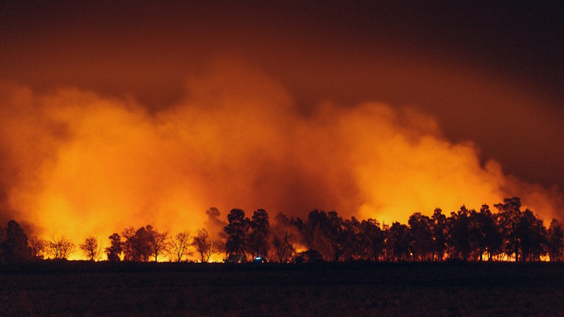
Fire Detectives In Orbit: Using Remote Sensing to Detect Wildfires
Iridian provides cost effective, advanced optical technology to enable optical Earth Observation (EO) and Remote Sensing for the purpose of wildfire detection, tracking, and management. Contact us for a customized solution to fit your needs.

Iridian to Visit OFC 2025
Iridian will be visiting OFC 2025 on April 1-3 at the Moscone Center in San Francisco, California, USA. We look forward to seeing you there! Click for more details.