The surface figure and wavefront distortion requirements for optical filters are highly dependent on the application / on where and how they are used. Whereas band-pass or clean-up functionality may only require control of the transmitted wavefront, dichroic beam-steering/splitting filters or wavelength selective mirrors often require specification of both the transmitted and reflected beams. Filters used in sensing applications with very tolerant detector geometries may not need, in practice, to put any constraints on the surface figure or wavefront distortion. It is important to understand where, when, how, and to what level to specify wavefront distortion to ensure that functional requirements are guaranteed while avoiding unnecessary and costly constraints.
What is Surface Figure/Flatness?
Surface figure encompasses the specification of the geometry of the two optical surfaces of filters with respect to each other and the resultant physical effect on the transmitted or reflected light. Flatness is a subset of surface figure specifying the geometry of a single surface. Flatness is often employed as a default catch-all parameter, used when there is uncertainty of the wavefront control requirements of a filter but the specifier knows (or at least believes) that it is necessary to specify something to avoid getting a highly curved optic that might distort the light path. The flatness of a surface is the maximum deviation from a perfectly flat surface of the same lateral dimensions specified in nm of deviation or sometimes as a “λ/XX @ YY nm” value ratio of the nominal wavelength used to characterize surface figure (typically 633nm). As such, this specification is influenced exclusively by geometric surface deviations of the filter. This spec only defines a single surface therefore flatness should be specified for both optical surfaces of the filter in question.
Flatness is commonly misused in specifying filters as it is purely a physical parameter of a single surface and is not wholly responsible for what really affects functionality – the maintenance of the quality of the wavefront and direction of the incident beam; i.e. its transmitted and reflected components. Optical filters will often include specifications for any or all of flatness, transmitted wavefront distortion or error (TWD/TWE), and reflected wavefront distortion or error (RWD/RWE), defined over the clear aperture of the filter or per unit of lateral dimension (e.g. per inch). In practice, specifying TWD and/or RWD should suffice. Usually flatness is not required as a filter spec (although it may be used to specify the uncoated substrates) and compensating for flatness with coatings can actually have a negative impact on TWD as we’ll show below.
What is TWD?
Transmitted wavefront distortion (TWD), or equivalently transmitted wavefront error (TWE), is a specification that describes deviation from a perfectly flat plane wave of the transmitted component of incident light. TWD is typically specified as a “λ/XX @ YY nm” value, the ratio of the nominal wavelength used to characterize surface figure (typically 633nm). TWD is important particularly in imaging applications as distortion of the transmitted beam can result in distorted images at the detector or variations in light intensity at the detector not resulting from the sample under test but rather a consequence of the influence of the filter itself.
TWD is influenced by the characteristics of the bare substrate prior to coating. Substrate parallelism specs influence TWD but inhomogeneity in the substrate material can also affect the transmitted wavefront due to variations in refractive index in the material. Similarly, effects from variations in coating uniformity can impact TWD, so consideration of the coating and substrate inhomogeneity on TWD is important especially in the case of thick, large, or complex filters.
What is RWD?
Reflected wavefront distortion (RWD) or equivalently reflected wavefront error (RWE) is a specification that describes deviation from a perfectly flat plane wave of the reflected component of incident light. RWD is typically specified as a “λ/XX @ YY nm” value, the ratio of the nominal wavelength used to characterize surface figure (typically 633nm). RWD is relevant for applications in which the reflected beam is used in imaging or detection as both the direction and distortion of the reflected wavefront are important.
Like TWD, RWD is influenced by the characteristics of the bare substrate prior to coating but, unlike TWD, the effect of coating stress often makes a very important contribution to RWD. Flatness of the primary reflective surface largely defines RWD so the flatness of the incident surface of the substrate matters. Stresses induced by complex coatings cause curvature of this surface. A perfectly flat substrate surface may be curved by the filter coating but can be flattened, at least partially, with an equivalently stressed backside coating (stress-balancing coating). Inhomogeneity in the substrate material is largely irrelevant as the reflected beam does not reach the substrate material itself but variations in coating uniformity can impact RWD.
Examples
The following figures illustrate different physical parameters such as individual surface flatness/curvature and substrate inhomogeneity and the resultant relative effects on TWD and RWD.
Figure 1: Flat, parallel, homogeneous substrate
Side A: flat; Side B: flat; Substrate: homogeneous
- TWD: low
- RWD: low
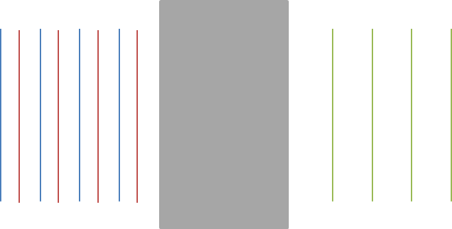
Figure 2: Curved, parallel, homogeneous substrate
Side A: curved; Side B: curved (same as side A); Substrate: homogeneous
- TWD: low
- RWD: high
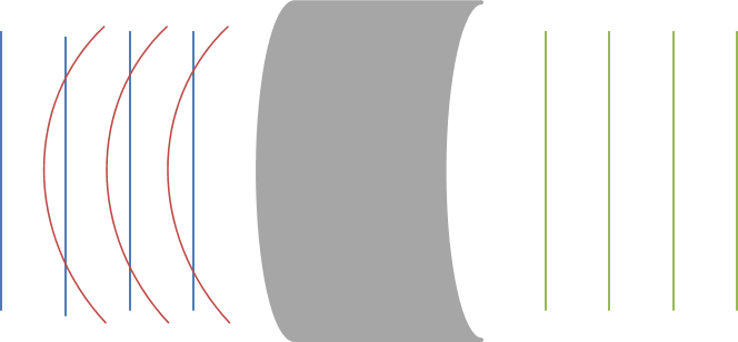
Figure 3: Curved, non-parallel, homogeneous substrate
Side A: curved; Side B: different than side A; Substrate: homogeneous
- TWD: high
- RWD: high
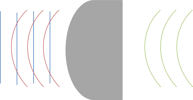
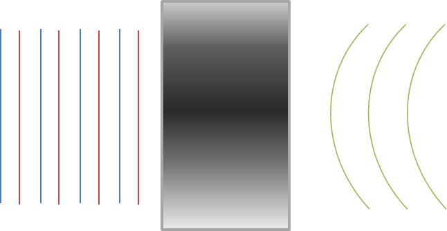
Figure 4: Flat, parallel, inhomogeneous substrate
Side A: flat; Side B: flat; Substrate: inhomogeneous
- TWD: high, RWD: low
Good Flatness ≠ Good TWD
Let’s look at an example illustrating how specifying flatness is not only not sufficient to ensuring good TWE values, but targeting low flatness values on coated parts can actually result in high TWE values.
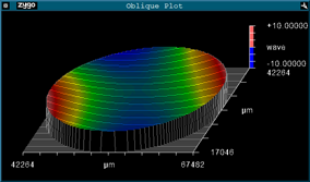
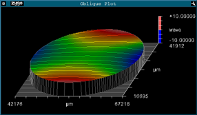
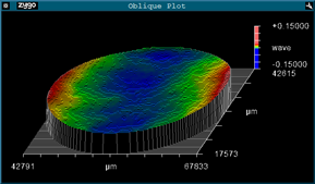
Here are interferograms showing flatness of each side of a “flat” uncoated substrate along with the corresponding TWE:
Flatness Side A (388nm Peak-to-Valley (p-v)):
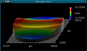
Flatness Side B (333nm p-v):

TWD (26nm p-v):
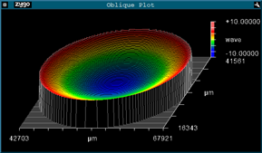
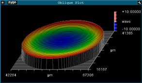
Here is the same substrate after a uniform coating on Side A. The substrate is now curved due to the stress induced by the coating but the TWD remains relatively unaffected:
Flatness Side A (7541nm p-v):
Flatness Side B (7569nm p-v):
TWD (30nm p-v):
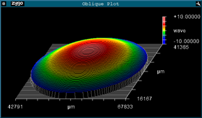
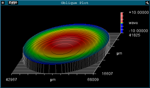
Finally, here is the same substrate after receiving a stress balancing coating on Side B to compensate for the curvature induced by the coating on Side A. Note, that the stress balancing coating was intentionally adjusted to highlight the effects of a non-uniform coating. The substrate is now significantly flatter compared to after the side A coating, but the increased coating thickness has degraded the TWD:
Flatness Side A (1417nm p-v):
Flatness Side B (1386nm p-v):
TWD (129nm p-v):
Here is a table showing these three cases side by side.
| Flatness Side A (p-v) | Flatness Side B (p-v) | TWD (p-v) | |
|---|---|---|---|
| Uncoated | 388nm | 333nm | 26nm |
| Side A coated | 7541nm | 7569nm | 30nm |
| Stress balanced | 1417nm | 1386nm | 129nm |
While low flatness values do have a correspondence with low RWD, as we can see in this example this is not the case with TWD and, even worse, pushing for low flatness (a physical parameter) can have negative consequences for TWD (a functional specification).
What to specify and when: cost and complexity implications?
While it may be tempting to specify all of flatness, TWD, and RWD as part of a complete filter specification, it is important to ensure that functionally irrelevant parameters are not specified as this can unnecessarily drive complexity and cost of filter builds.
TWD specs largely drive substrate parallelism and homogeneity specs so are tied to the sourced material costs; from the perspective of the optical filter manufacturers these specs gets passed along to substrate manufacturers and the resultant costs to the requesting customer.
On the other hand, RWD specs influence both the raw substrate costs (specified as flatness requirements for the uncoated substrates) and, perhaps more significantly, the filter coating run times, yields, and costs due to the requirements to control, understand, and compensate for the curvature induced by the filter coating through stress balancing coatings often as thick as the primary coating. Additionally the added stress balancing coating can have a negative effect on other filter specs such as surface quality due to additional handling and longer coating times potentially generating more defects.
Here are a few guidelines for when to specify TWD and/or RWD:
- Filters used at normal (0 degrees) angles of incidence:
- Typical filter types: band-pass, edge-pass, notch
- Typical applications: imaging
- In these optical designs, for almost all cases, only the transmitted wavelengths are used and all other light can be considered to be “blocked” (rather than reflected even if that is how the blocking is achieved)
- RWD should not be specified (the reflected light is not recovered)
- TWD should be specified if preservation of the wavefront or direction of the transmitted light is important for the application
- Filters used at non-normal (often 45 degrees but any values >0) angles of incidence:
- Typical filter types: dichroic or ratio beam-splitters, mirrors
- Typical applications: multi-wavelength imaging, beam-steering
- In these optical designs often both the transmitted and reflected wavelengths are used (or in the case of mirrors only the reflected wavelengths)
- RWD should be specified if the reflected light is to be recovered/used
- TWD should be specified in the case of beam-splitters if preservation of the wavefront or direction of the transmitted light is important for the application